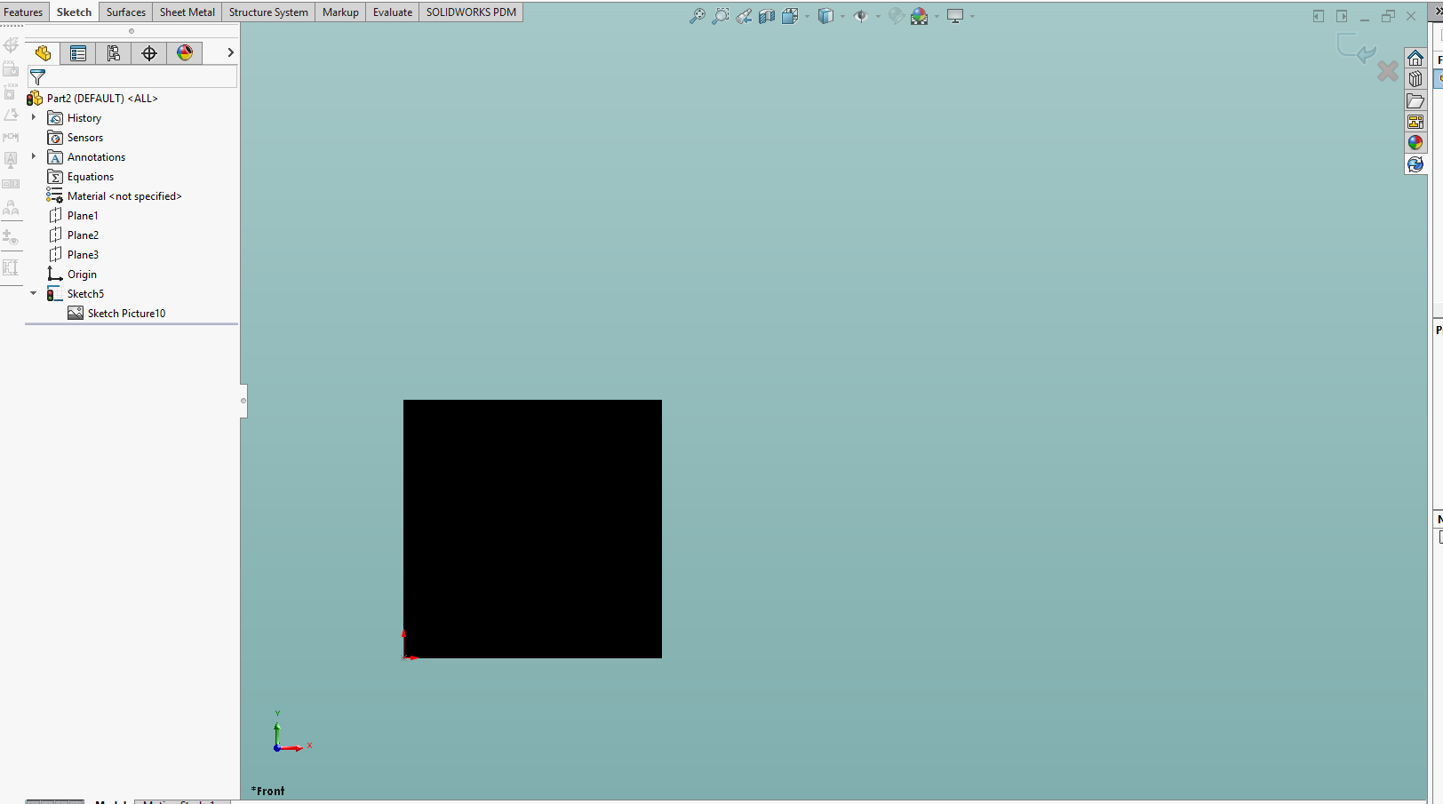
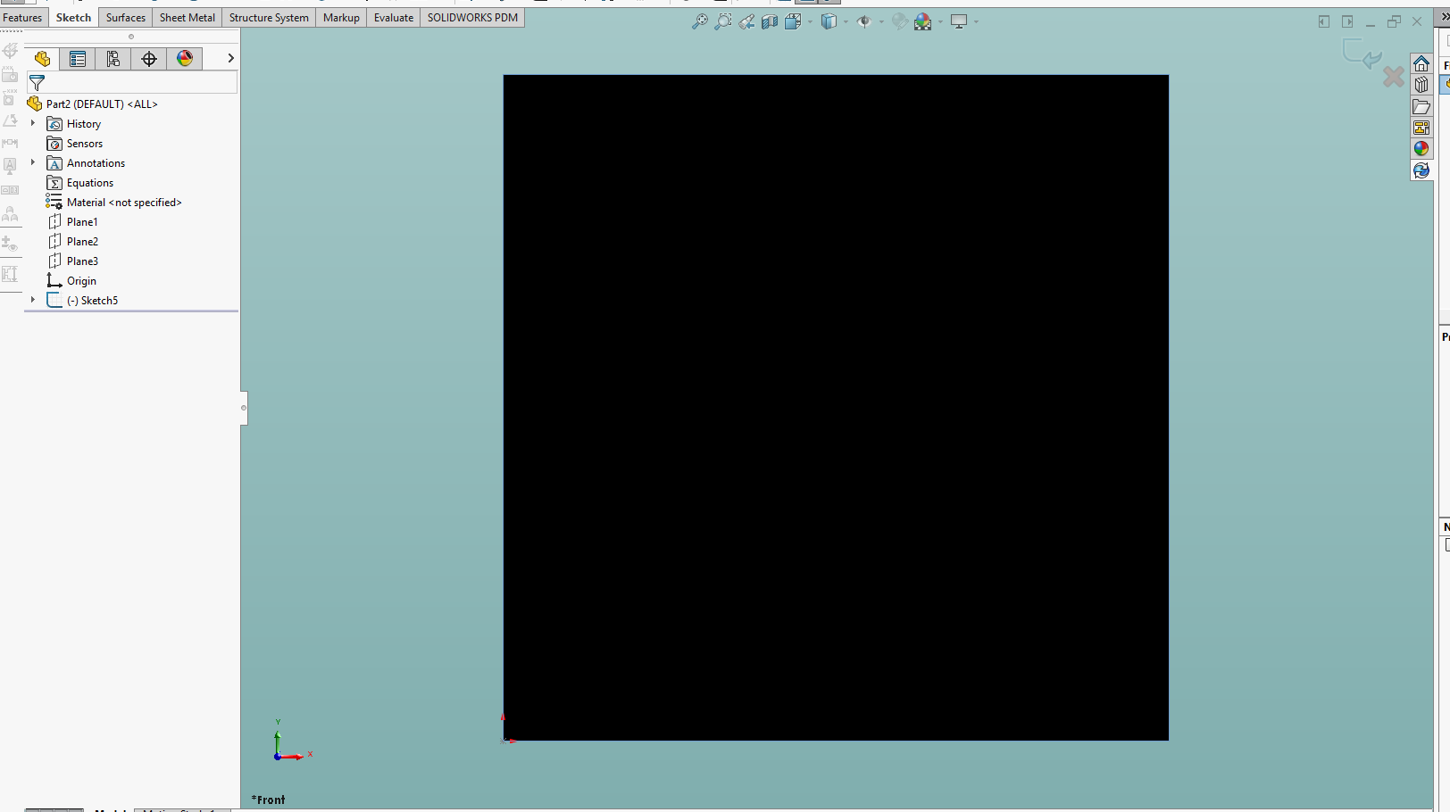
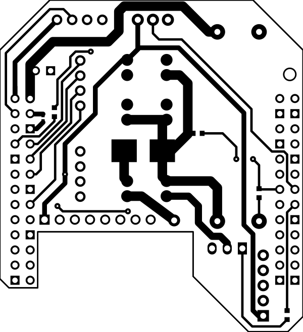
In my models I often need to include a sketch picture. It appears that when you import a picture, SW initially treats 1 pixel = 1mm for scale. Like for example, this picture is 600x658px, so when imported, it’s default size is 600x658mm:
Of course, I can re-scale it, in this case it should be 50.8x55.7mm:
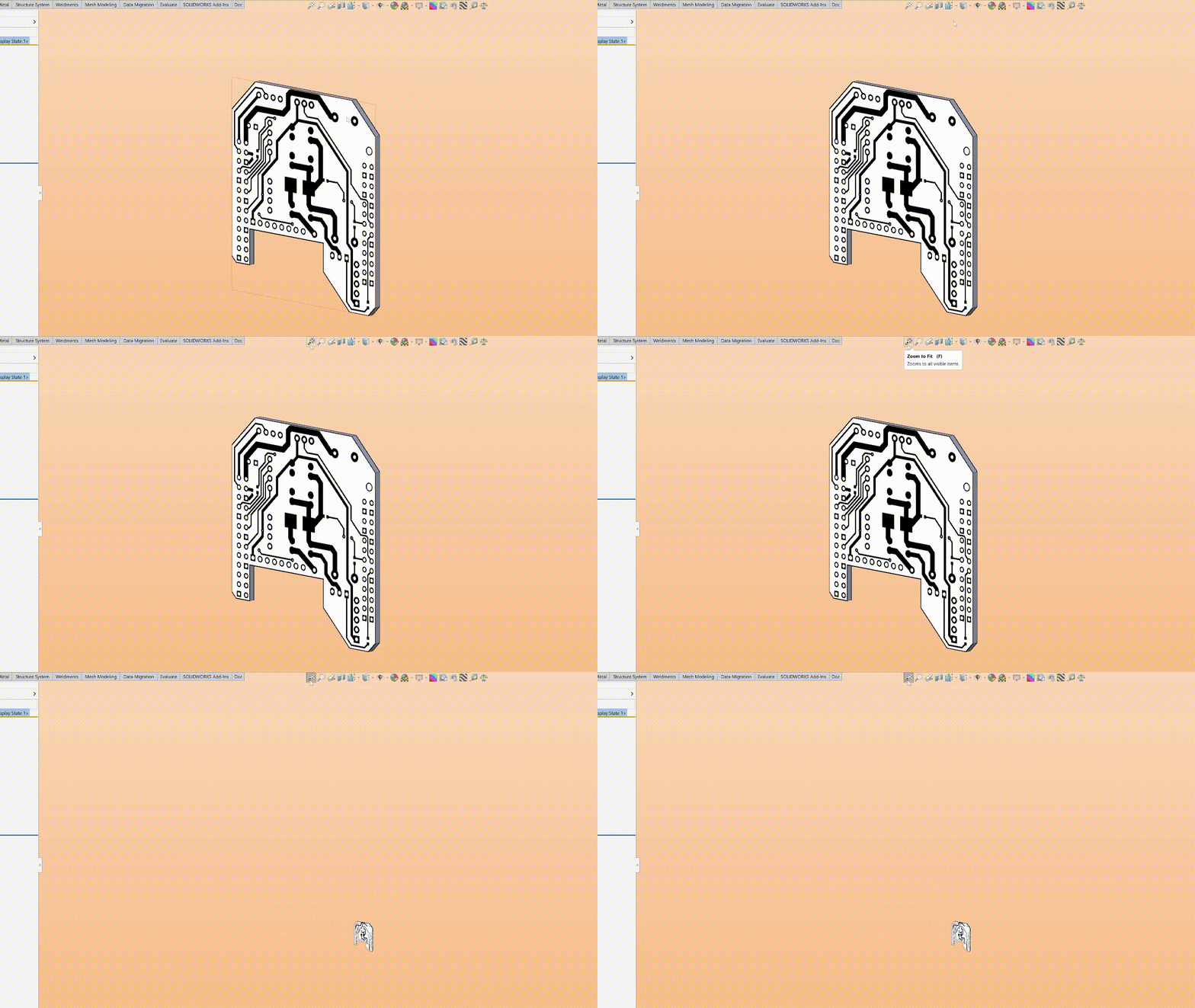
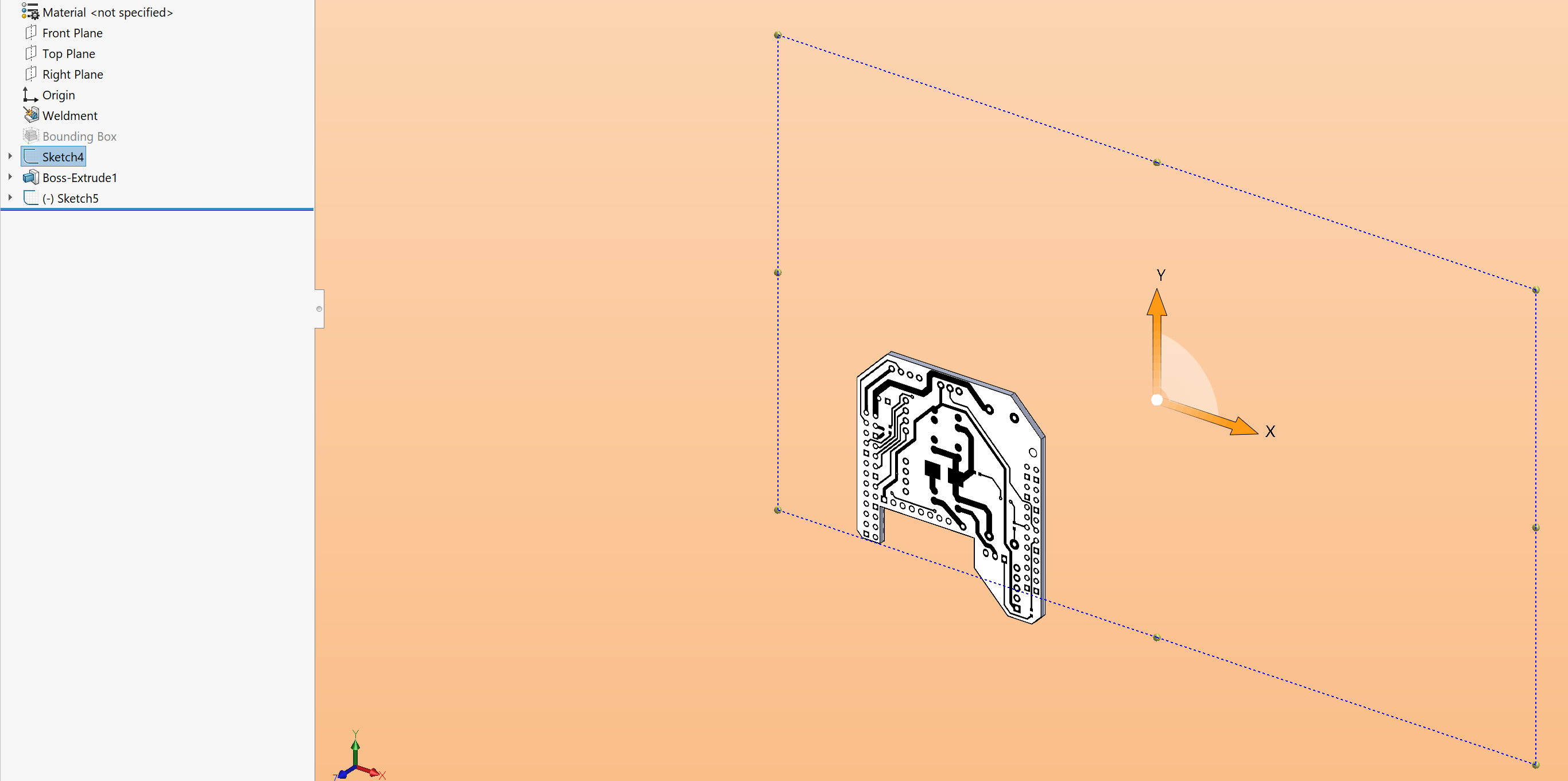
However, even after sketch is saved, lots of weird behavior remains. For example, zoom to fit zooms the part waaay past it’s extents:
Lot of other shenenigans as well: part file thumbnail becomes zoomed out too. When using this part in assembly, selection around the part becomes weird, you click some other part but the part with picture gets selected. And so on.
It seems that for whatever reason SW still thinks that picture is larger than it actually is, which messes up visual bounding box and selection stuff.
The only way I found to fix this is to reduce image size before importing to the correct one, but in my case that would be 50x56px, which is horrible quality image. Unfortunately SW doesn’t seem to acknowledge the DPI setting of the image.
The scale tool construction line is taken into consideration when zooming to fit and such. Make sure you turn it off, or move it somewhere within the bounds of the part geometry.
Exit sketch and zoom to fit. The image remains shifted toward the bottom left if the view area.
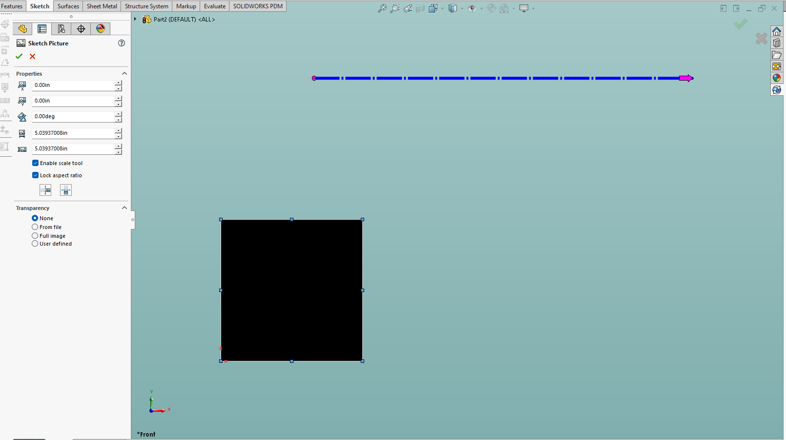
Edit the sketch and double click the picture. The scale line is displayed and it is above and to the right of the image (basically at the image center before it was scaled):
Well that is super weird. I tried the exact same thing, but it isn’t working for me. Attaching the file. Not sure which version you’re on, I’m on 2024, so I backported to 2022. Also attaching the image file separately.
You model file misbehaves for me in SW2025. If I take you image file and use it in a new SW2025 model file, it behaves. If I use my image file in your model, it misbehaves. I took my 2025 template and saved it as as a SW2024 part file and with your image it behaves.
So, it appears that something is wrong with that specific part file, or your part template. I’ve attached my 2024 part file for you to try out.
This is with Instant3D turned on. Turns out, you can resize that rectangle by dragging on the corners. And apparently it is accounted for in zoom to fit function. I moved the corners of this rectangle to make it smaller than the part, and zoom to fit now behaves properly.
Now what does that rectangle mean, I have no idea. I know that the arrows in the middle are meant for moving undefined sketches, and that rectangle is bounding box perhaps? But the sketch is empty, except for the picture, which is far smaller than the bounding box. Maybe that box was created initially when I first imported the picture, and it doesn’t get updated afterwards. One more SW quirk…
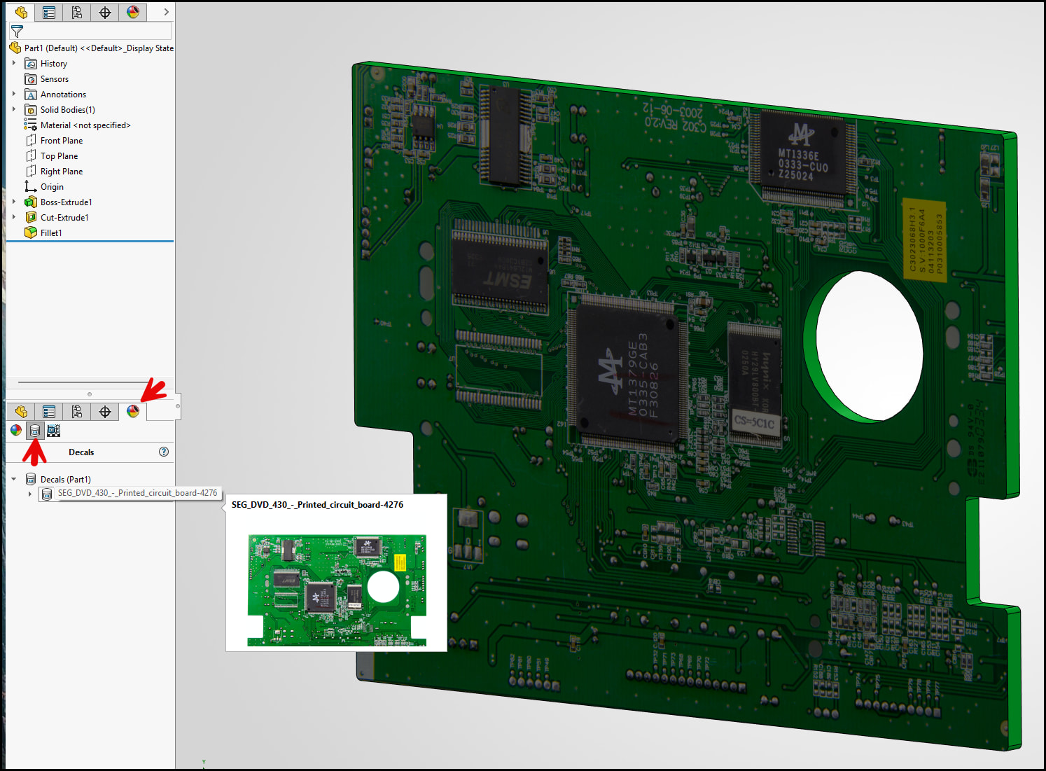
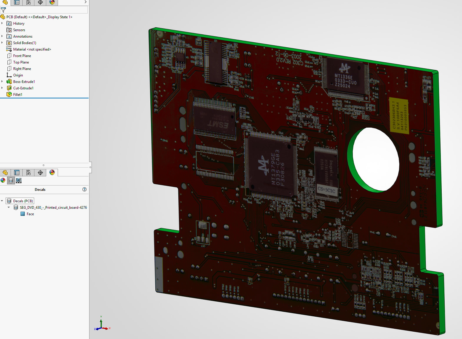
Yeah, I guess I’ll use decal too. Don’t have much experience with these. Glad to see I’m not the only one who does PCBs like that lol. Does the decal keep a parametric link to the image file? I keep updating these layouts like 20 times an hour.
It allows you to scale sketch geometry that isn’t constrained in X or Y. As soon as you add a relation or dimension that pins anything down, it won’t even show up anymore. Seems pretty useless to me.
Nice. By the way, what PCB design tool are you using? I’m still stuck with EasyEDA, mostly because of the community library, can find almost anything there (with other tools there were always some missing components that I would have to recreate myself, and got tired of it). Unfortunately it does not work with CircuitWorks, which is why I have to do all of the component placement based on these pictures…
I rescale and edit images using Affinity software which is a Photoshop competitor, now a free to use software. I can scale the image in inches or mm to create an outline that matches the size of the part.
I haven’t figured out a way to use CircuitWorks with Altium. The export options in Altium doesn’t have the options that CW uses. There was an Altium connector you can purchase but we never did buy it.
We also tried getting STEP files from Altium but its too heavy as we get thousands of bodies for tiny components. Just way to much detail as well fairly large assemblies they go into.
If I remember it right, CircuitWorks needs IDF file which Altium can export. Then it’s basically loading up CircuitWorks addin, then in menu going to Tools → CircuitWorks → Open ECAD file, selecting that IDF, and then it searches it’s component library for the components on that PCB. If it finds it, it uses them, otherwise it draws boxes based on bounding box data of each component. If you need accuracy you might need to map components you use to the CW library parts. There is a tutorial on this in Help → Advanced Topics → CircuitWorks.
This is as far as I remember. Haven’t used it myself because like my ECAD doesn’t export IDF.