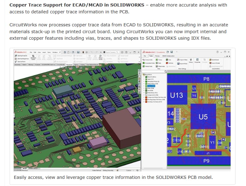
I see that Circuitworks 2025 introduced copper trace support from IDX files. Has anyone actually tried this in practice and does it work as you’d like it to?
How is it being added to the model? If its creating an extrude or split face then I’d say no, we wouldn’t use something like that. Today we insert an image of the PCB (Altium) as a decal so it looks correct.
1 Like
I think it comes in as a surface. Hopefully loading up an install of SW25 in the next couple of weeks to do a test on it.
Where many of our boards need lids for RF shielding it would be useful to be able to create sketches from the top layer copper geometry in order to produce the lid walls. Right now we use decals to show and then have to do a LOT of manual edge aligning to make the wall geometry.
We would want to avoid extra edges for performance, especially on the drawing.
